
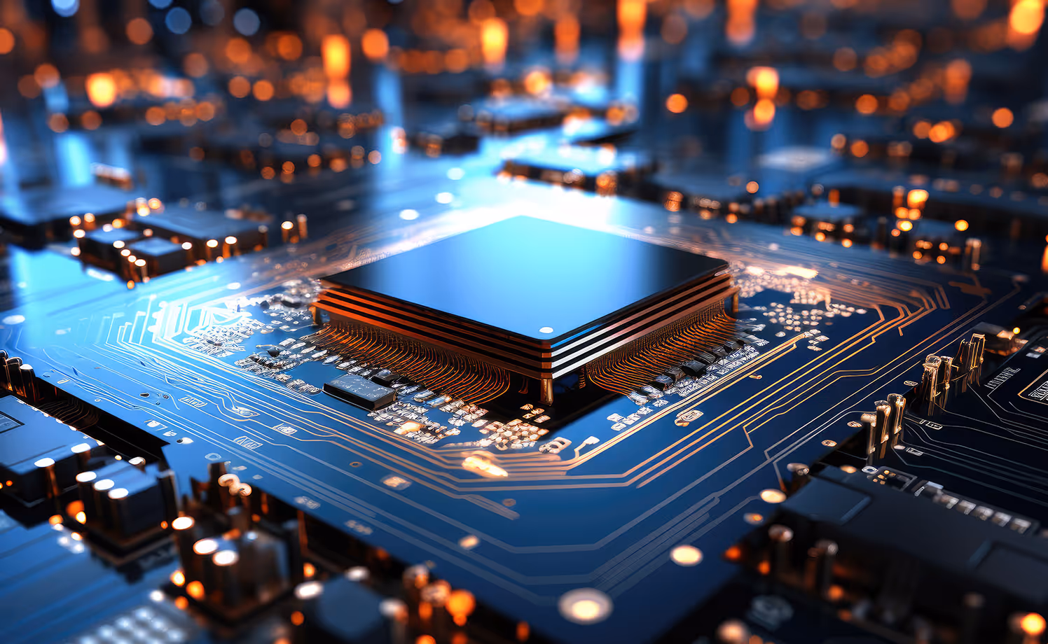
In the world of contemporary technology, Printed Circuit Boards (PCBs) are essential components in almost every electronic device human beings use regularly. Whether it’s smartphones, laptops, medical devices or automotive systems, PCBs play a vital role in ensuring the functionality of numerous electrical and mechanical devices. Despite their widespread use, understanding PCB design can still be a challenge for aspiring engineers. This article dives into the intricacies of PCB design, breaking down its complexities to empower individuals with foundational knowledge.
The Printed Circuit Board (PCB) is a crucial component underlying the functionality of most modern electronic gadgets. It acts as a central hub for connecting electronic parts within a device, providing both electrical pathways and mechanical support. Essentially, physical circuit boards are built from insulating materials, usually plastic or laminate, embedded with a.o. integrated circuits and copper traces. These pathways establish electrical connections between various electronic components like transistors, resistors, capacitors and diodes.Beyond just connections between components, PCBs enable the optimization of electronic layouts for performance, size and cost-effectiveness. The circuit boards are designed to be versatile and suitable for various applications, which is especially advantageous in mass-producing electronic devices, where standardizing circuit designs can significantly cut manufacturing expenses.The Importance of Precision in Printed Circuit BoardCrafting precise PCB design solutions hold paramount importance in ensuring the optimal performance and reliability of many electronic devices. It involves fine-tuning signal trace lengths, bolstering interference resilience and mitigating assembly inaccuracies, all of which are pivotal for seamless functionality. Moreover, strategic component placement and the integration of thermal layers serve to thwart overheating issues, thereby prolonging the device’s operational lifespan. Investing in precise PCB design and manufacture can yield products distinguished by superior quality, enhanced efficiency and heightened dependability.
The design procedure and its vital components comprise:
The PCB conceptualization process holds significant sway over the performance and functionality of electronic apparatuses. Proper PCB conceptualization can expedite time to market, amplify system reliability and curtail production expenses.
One of the crucial factors in ensuring the reliability of devices is the effective management of temperature. This is supported by the careful selection of appropriate insulating materials. Dielectric materials with notable thermal conductivity can facilitate the swift dissipation of heat. The strategic arrangement of components, employing a multi-layered structure for the printed circuit board and judicious utilization of copper layers also contribute to efficient heat dissipation beyond the confines of the device casing. Excessive clustering of components or improper PCB layering might lead to the accumulation of heat and subsequent overheating of the circuitry. Equally significant are the thermal pathways. Their meticulous design facilitates the efficient transfer of heat from critical areas to cooling zones, such as copper planes on the PCB or a heat sink. Furthermore, rigorous testing and thermal verification are imperative. Thermal evaluations assist in pinpointing areas with heightened heat concentration and potential overheating zones. As a result, designers can make necessary adjustments to their designs, ensuring optimal operational conditions for all components.
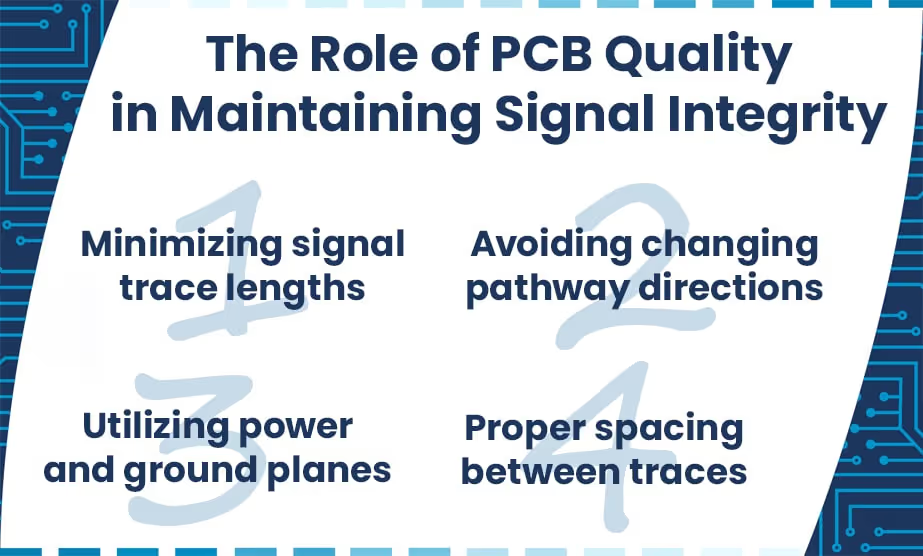
To ensure signal integrity InTechHouse design teams always follow several key routing principles during PCB design:
The initiation of a sturdy project involves careful planning and thorough analysis of requirements. Subsequently, the careful selection of suitable materials follows. While top-quality components may result in higher initial expenses, they generally lead to decreased failure rates and extended operational lifespans. Designers should choose materials resistant to external factors such as moisture, temperature variations or mechanical strains.Furthermore, the strategic integration of advanced technologies is of significant importance. For instance, utilizing modern manufacturing techniques like additive manufacturing or precise laser machining enables precise component fabrication while reducing the risk of manufacturing defects. Additionally, ergonomic and usability considerations have a substantial impact on the device’s durability and continued usefulness over time. Lastly, rigorous testing is imperative.
There are the main principles that help a PCB designer achieve optimal component placement to improve, especially device speed and efficiency. Remember to:
InTechHouse has also some tips on how to enhance the power efficiency of the device thanks to PCB design:
Moreover, implementing straightforward methods to facilitate board flexibility and scalability involves:
In the latest time PCB manufacturers are increasingly prioritizing the creation of PCBs that excel not only in performance but also in their eco-friendliness. It’s possible to achieve this using a flax-fibre-based composite.Another notable technological trend in PCB manufacturing is the emergence of high-density interconnect (HDI) technology. HDI has evolved alongside every layer interconnect (ELIC) and any layer interconnect (ALIC). This advancement addresses the increasing need for faster and more compact methods of interconnecting devices. HDI enables manufacturers to mass-produce smaller wireless products capable of rapid signal transmission, enhanced routing capabilities, and reduced power consumption.
The most frequent design errors:
Best practices and strategies for avoiding these common pitfalls:
Apple: In products such as the iPhone and MacBook, Apple utilizes advanced PCB design technologies to achieve incredibly compact sizes while ensuring high performance and reliability.Tesla: In Tesla electric vehicles such as the Model S and Model 3, leading PCB design allows for the integration of advanced electrical, multimedia and safety systems, impacting both the appearance and reliability of the vehicles.Medtronic: As a leader in medical technology, Medtronic utilizes complex integrated circuit boards in devices such as pacemakers, insulin pumps and neurological treatment devices, ensuring reliability and patient safety.Conclusion? It’s not worth investing in low-quality components. Instances of poor PCB design primarily impact a company’s reputation and brand image. Low-quality components discourage consumers, leading to increased device defects. More frequent complaints also necessitate costly repairs or even the replacement of entire electronic circuits. PCBs of poor quality can limit device performance by impeding the flow of energy or data between various electronic components. They can also lead to various types of faults, such as short circuits, track breaks or instability in electronic systems.
In conclusion, mastering the basics of PCB design is not merely a technical endeavor but a gateway to unlocking the full potential of the modern electronics industry. By unraveling the complexities of PCB design and adhering to best practices organizations can rise to a higher level.InTechHouse is the best team of experts in PCB design. We deliver top-notch solutions for businesses in hardware, software and embedded systems.Interested in collaborating? Feel free to reach out to us.
Some of the most popular ones are: Altium Designer, Eagle and KiCad.
DFM considers manufacturing processes and limitations early in the design phase to minimize production issues and reduce costs.
DRC ensures the design meets specified constraints, such as minimum trace widths, clearance and solder mask tolerances, to ensure manufacturability and reliability.
Techniques such as controlled impedance routing, minimizing signal reflections, and proper grounding and power distribution help maintain signal integrity.
A technology leader specializing in advanced hardware, embedded systems, and AI solutions.
He bridges deep engineering expertise with strategic thinking, helping transform complex system architectures into practical technologies used across industries such as aerospace, defense, telecommunications, and industrial IoT.
With a strong engineering background and ongoing PhD research, he combines academic insight with real-world project experience. Jacek also shares his knowledge through technical and business publications, focusing on system design, digital transformation, and the evolving integration of hardware and AI.
This initial conversation is focused on understanding your product, technical challenges, and constraints.
No sales pitch - just a practical discussion with experienced engineers.
Share a few details about your product and context. We’ll review the information and suggest the most appropriate next step.