
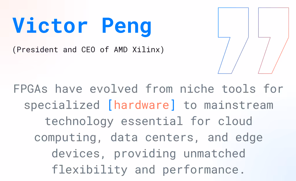
Field Programmable Gate Arrays (FPGAs) services have become a critical technology in the hardware domain, especially in industries that require high performance, low latency, and flexibility in hardware designs. Though FPGAs have existed for several decades, advancements in their capabilities and applications have made them more relevant today. As Victor Peng, President and CEO of AMD Xilinx, emphasizes, "FPGAs have evolved from niche tools for specialized hardware to mainstream technology essential for cloud computing, data centers, and edge devices, providing unmatched flexibility and performance". This article dives into the use FPGAs, how they work, and with what challenges struggle.
An FPGA is an integrated circuit (IC) that can be configured by the user after manufacturing, hence the term "field-programmable." Unlike fixed-function Application-Specific Integrated Circuits (ASICs), which are custom-designed for a specific task, FPGAs are reprogrammable and can be configured to perform different logic operations or functions. This makes them highly versatile for various applications across industries.
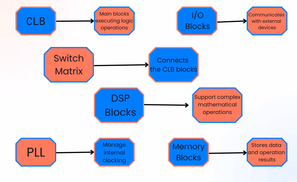
FPGA is an advanced architecture offering immense flexibility for creating complex digital systems. Understanding the construction of FPGA is essential for professionals aiming to fully leverage its potential in hardware design.
At the core are the CLBs, which are much more than just standard logic gates. These blocks contain:
Each CLB is fully configurable, meaning the FPGA can be dynamically adapted to a wide range of tasks, from signal processing to implementing AI algorithms.
The network of programmable interconnects is the true power of FPGA. While the CLBs define what the circuit does, the interconnects determine how the CLBs communicate with each other. This programmable infrastructure allows precise control over data flow and logic, enabling both simple combinational logic and complex multi-level structures. This makes FPGAs a versatile platform – they can be reconfigured on the fly for different applications, which is invaluable in areas such as adaptive signal processing or dynamic resource management in networks.
Flexible and efficient I/O modules enable FPGA to integrate with a wide range of external devices, from high-speed DDR4 memory to high-bandwidth interfaces like PCIe, Ethernet, or HDMI. With configurable signal standards, FPGAs can handle various protocols, making them ideal for complex embedded systems or real-time systems.
Modern FPGAs come equipped with dedicated memory blocks like SRAM or BRAM, allowing local data buffering without the need for external memory. These integrated low-latency RAM blocks are perfect for data-intensive applications such as machine learning algorithms or fast cryptographic algorithms.
High-end FPGAs often feature advanced DSP blocks optimized for tasks related to signal processing, such as signal filtering, FFT operations, or even convolutions in neural networks. DSP blocks allow the direct implementation of complex mathematical operations without burdening the general logic of the circuit, speeding up processing time and minimizing resource usage.
PLLs are invaluable tools for precise clock management in FPGA. PLLs enable the generation of multiple clock signals at different frequencies, which is crucial in systems requiring synchronization of many components, such as multi-band systems or IoT devices managing various communication interfaces.
At the core of FPGA's programmability is the configuration interface, allowing dynamic loading of the bitstream. Through JTAG, SPI, or other interfaces, users can quickly reprogram the FPGA, enabling real-time system reconfiguration. This feature makes FPGA unique in applications requiring high flexibility, such as adaptive systems, networking devices, or compute servers dedicated to specific algorithms.
FPGA programming is an advanced topic that requires a deep understanding of digital hardware and familiarity with hardware description languages such as VHDL or Verilog. Unlike traditional software, which runs on sequential processors, FPGA programming allows for the design of custom, highly parallel hardware architectures, resulting in exceptionally high performance and low latency in tasks requiring real-time processing. FPGA developers must think in terms of parallel data processing, breaking down algorithms into logical blocks, and optimizing signal paths. This process includes HDL code synthesis, mapping logic to hardware resources, and timing analysis to meet strict timing requirements. Unlike traditional ASIC design, FPGAs offer the advantage of reconfigurable hardware after deployment, enabling functionality updates or adjustments to changing system requirements without the need to manufacture new chips. Additionally, the integration of DSP blocks, RAM, and external interfaces enables the creation of more advanced and complex designs. As a result, FPGA programming is crucial in areas such as signal processing, AI algorithm acceleration, high-speed network protocol implementation, and cryptographic applications. Thanks to modern EDA (Electronic Design Automation) tools, this process has become more automated, enabling faster design iterations and more precise verification of functionality and performance optimization at the hardware level.
FPGA and ASIC are often compared because they serve similar functions but have distinct characteristics. The choice between them typically comes down to key project requirements such as flexibility, cost, time to market, and performance.
Features
FPGA
ASIC
Reconfigurability ability
Yes
No
Performance
Lower
High
Energy efficiency
Lower
High
Unit cost
Higher
Lower
Design cost
No NRE
High NRE
Time to market
Shorter
Longer
Prototyping
Available after production
Lack of post-production capability
Production scalability
Cost-effective for low to medium production scale
Cost-effective only for large-scale production
Tab. 1 Comparison FPGA and ASIC
More about differences between FPGA and ASIC you can read here: https://intechhouse.com/blog/asic-vs-fpga-which-soc-solution-is-right-for-your-next-project/
Due to their flexibility, FPGAs are used across a wide range of industries. Below are some of the most notable applications:
A technology leader specializing in hardware and embedded systems.
He has extensive experience delivering complex engineering projects for industries such as energy, military & defence, and aerospace.
His work centers on developing reliable, high-performance hardware systems designed for demanding environments and long-term industrial deployment. Adam combines deep technical expertise with practical engineering leadership, helping transform advanced embedded technologies into robust, mission-critical solutions used by global clients.
This initial conversation is focused on understanding your product, technical challenges, and constraints.
No sales pitch - just a practical discussion with experienced engineers.
Share a few details about your product and context. We’ll review the information and suggest the most appropriate next step.