Modern electronics is evolving toward ever higher data transmission speeds and greater component density. What just a decade ago could be treated as a simple matter of correctly connecting integrated circuits with conductive traces is no longer sufficient. Today, it requires an approach that accounts for wave phenomena, signal integrity (SI), and power integrity (PI). So how can designers ensure that their high-speed circuitry remains both reliable and efficient?
This article presents seven key rules that help designers maintain control over critical aspects of high-frequency systems. The goal is not only to outline theoretical guidelines. It is also to provide practical recommendations which, when implemented already at the schematic layout stage, help avoid costly mistakes above all.
Need Professional PCB Design Services?
Our Hardware Design team has over 10 years of experience designing PCBs for automotive, medtech, and IoT industries. We offer comprehensive services – from concept to production.
At frequencies in the hundreds of megahertz, the length of a PCB trace starts to become comparable to the wavelength of the signal. As a result, reflections, attenuation, and phase shifts occur, which can disrupt data transmission or even completely prevent an interface from functioning correctly. Equally important are the dielectric parameters of the laminate, such as the dielectric constant (Dk) and dissipation factor (Df), which influence signal propagation and losses. Choosing the right PCB material therefore takes on strategic importance and often determines the success of the circuit design process.
“Choosing the right laminate is one of the first strategic decisions in high-speed design. A wrong Dk value can ruin your signal integrity before you even start routing.” – Lee Ritchey, Founder of Speeding Edge
Another area of concern involves electromagnetic issues. Higher frequencies generate stronger emissions, while at the same time making the system more susceptible to external signals. This is why high-speed PCB design and layout must integrate electromagnetic compatibility (EMC) analysis and immunity testing.
The manufacturing aspect also cannot be overlooked. Technologies such as microvias, multilayer laminates, controlled dielectric thickness, and reliable solder processes are necessary to meet the requirements of modern interfaces such as PCIe, DDR, HDMI, or USB 3.x. This means that the designer must work closely with the PCB manufacturer to ensure that theoretical assumptions can be translated into practical board layout and production.
All these factors make high-speed PCB design a system-level discipline. Every detail, from materials and trace geometry to the fabrication process, has a direct impact on the final reliability and performance of the device.
Discover our ranking: The best EMC testing companies in the EU:
https://intechhouse.com/blog/essential-guide-to-emc-testing-ce-certification-for-compliance-success/
In high-speed PCB design, one of the most important aspects is maintaining a consistent characteristic impedance of signal traces. This impedance describes how a signal “sees” a given transmission line and depends on several factors, including:
If the impedance does not match the value required by the interface (e.g., 50 Ω for single-ended signals or 100 Ω for differential pairs), reflections occur in the circuit, leading to waveform distortion and potential data loss.
A key factor is the selection of trace width and copper thickness. The wider the trace, the lower the impedance; meanwhile, greater copper thickness increases the conduction area, which also affects the result. Reducing the distance to the ground plane lowers impedance, while a thicker dielectric layer increases it. All of these parameters must be chosen so that the target impedance value is maintained for a given layer and laminate material.
Ultimately, impedance control is not just a theoretical concept but a practical requirement for the reliable operation of interfaces. Therefore, every high-speed project should begin with clearly defined impedance requirements and close collaboration with the PCB manufacturer to ensure that tolerances are maintained during production.
What should be kept in mind when designing high-speed PCBs? One of the most critical factors is signal propagation delay. An electrical signal does not travel at the speed of light in a vacuum but at a velocity determined by the dielectric properties of the PCB laminate. Typically, this is about 40–70% of the speed of light, which means that even a few extra centimeters of trace length can generate noticeable delays. At high frequencies, these differences translate into clocking errors, asynchronous communication, and loss of data integrity.
Industry trends underscore the growing importance of this. The high-speed PCB market is expanding at a CAGR of around 12% annually, with designs for 5G, IoT, and automotive applications already requiring handling signals above 10 GHz. In such environments, even small mismatches or extended critical traces can make the difference between stable operation and complete system failure.
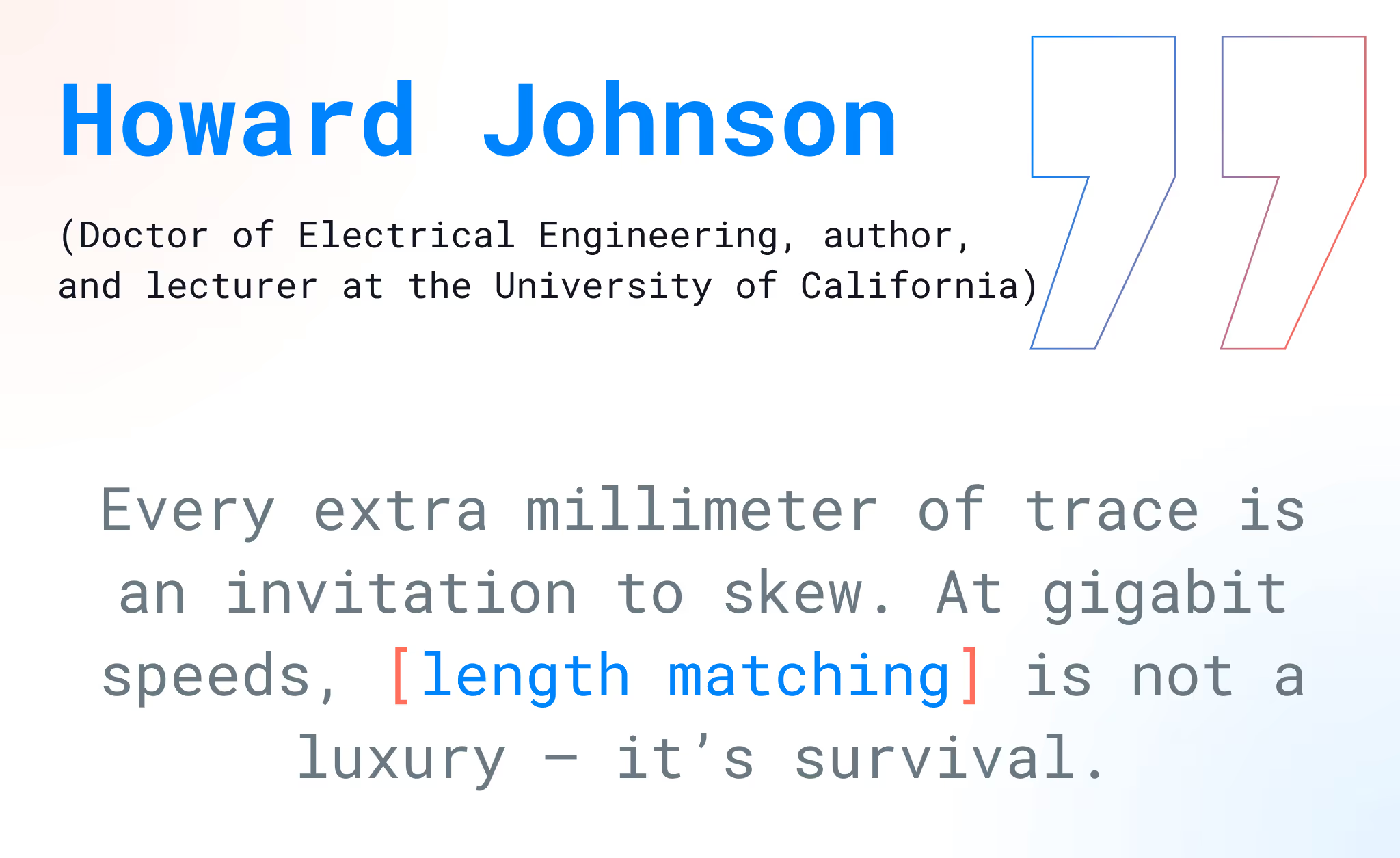
The effects of extended connections are especially evident in interfaces that require multiple signals to be transmitted simultaneously, such as DDR memory buses, USB data lines, or clock signals. If one signal reaches the receiver earlier than another, a phenomenon known as skew occurs, which is a timing mismatch between lines. Even small differences on the order of hundreds of picoseconds can result in incorrect data interpretation and destabilization of the entire system.
Long traces also carry other risks: increased signal attenuation, greater susceptibility to external interference, and higher likelihood of electromagnetic emissions. In practice, this means that critical traces (those carrying clock, high-frequency, or synchronization signals) should be routed as short and as straight as possible. Unnecessary bends and layer transitions should be avoided.
However, minimizing length alone is not always sufficient. Designers must also ensure length matching between parallel signal lines so that signals arrive simultaneously. That is why EDA software provides automatic length-matching features, which help maintain timing consistency across entire groups of signals.
Ultimately, shortening and controlling the length of critical traces is not just good design practice but an essential requirement for the reliable operation of high-speed systems.
In high-speed PCB design, one of the common issues is also crosstalk, which refers to unwanted coupling between adjacent signal lines. This effect becomes more pronounced as signal frequency increases and as traces are routed in parallel over longer distances, leading to waveform distortions, increased jitter, or random transmission errors.
The primary preventive measure is maintaining proper spacing between high-frequency signals. A practical rule states that the greater the spacing between lines, the weaker the coupling. In many design standards, the “3W rule” is applied—the spacing should be at least three times the trace width. In critical cases, such as clock lines or differential pairs, even larger separations are recommended. Where possible, signals should also be routed in different layers separated by a ground plane.
The most important techniques for reducing interference include:
Avoiding crosstalk is not only a matter of signal quality but also of meeting electromagnetic compatibility (EMC) standards. Therefore, proper trace placement, adequate spacing, and effective shielding techniques are fundamental to ensuring the stable and reliable operation of high-speed systems.
Ground planes serve a dual role: on one hand, they provide an electrical reference for signals, and on the other, they form a low-resistance return path for current. This minimizes current loops, reduces noise emissions, and improves the integrity of high-frequency signals. The absence of a continuous, uninterrupted ground plane leads to uncontrolled return paths, resulting in crosstalk, noise, and transmission errors that are difficult to diagnose.
Power planes are equally important, especially in modern systems that often operate at low voltages and high currents. A stable and well-designed power distribution network helps avoid voltage drops. It also ensures proper operating conditions for sensitive ICs such as processors, memory modules, and communication chips. Designers must also account for power integrity (PI) phenomena, ensuring that energy is delivered evenly across the PCB without generating interference.
In practice, several key design rules are applied:
A well-structured system of planes also simplifies stack-up optimization, allowing for a better balance between electrical performance and manufacturing cost.
Differential pairs are two traces carrying signals of the same frequency but with opposite polarities. This method of transmission provides strong immunity to noise, as any external interference induced in both lines cancels out at the receiver. However, for proper operation, certain geometric and timing parameters must be maintained, with the most critical being trace length matching.
“Differential pairs are unforgiving. Get the geometry wrong, and your 10-gigabit link becomes a 10-megabit headache.” – Lee Ritchey, Founder of Speeding Edge
A difference in length between the lines of a pair leads to what is known as skew, or a timing offset between signals. Even a very small difference—on the order of tenths of a millimeter—can cause incorrect data interpretation at gigahertz frequencies. For this reason, modern EDA tools include automatic length-matching functions, allowing designers to insert characteristic serpentine (meander) patterns in the shorter trace to equalize it with the longer one.
In addition to length, maintaining a consistent spacing between differential lines is equally important, as it directly affects the pair’s impedance. Common standards such as USB 3.x, HDMI, and PCIe require a differential impedance of around 90–100 Ω, which means the designer must precisely define both the trace width and the separation. It is also essential to route both lines in the same layer and avoid unnecessary vias, which can introduce asymmetry.
In practice, additional rules apply, such as keeping the lines parallel along their entire length, avoiding sharp corners, and ensuring that differential pairs share a common reference plane. Equally important is verifying that the connector footprint and pad geometry support the required impedance control. By following these principles, differential signals maintain synchronization and resilience against interference, ensuring stable system operation even at very high data rates.
Vias are elements that connect traces between layers. While they are an essential tool in building complex multilayer boards, each via introduces additional electrical effects that can negatively impact signal integrity. The most significant of these are parasitic inductance and capacitance, as well as the extension of the signal path, which results in additional attenuation and reflections.
At high frequencies, every via becomes a potential source of interference. Even a small impedance mismatch in the via region can cause unwanted resonances that distort the signal waveform. In high-speed interfaces, even a single poorly designed via can lead to communication errors. Therefore, the fundamental rule is to minimize the number of vias in critical signal paths.
If the use of vias is unavoidable, designers should follow several practices:
It is also important to remember that vias affect the signal’s return path. For this reason, ground stitching vias are often added near signal vias to ensure continuity of the reference plane and minimize current loops, while also improving overall manufacturability of the board.
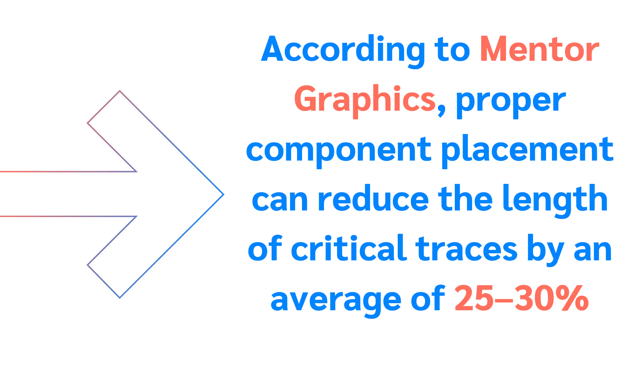
Proper component placement on a PCB is critically important in high-speed designs. This stage determines not only ergonomics and ease of assembly but, above all, signal integrity and the overall stability of the system. Incorrect placement of components can result in longer traces, uncontrolled ground loops, and increased susceptibility to electromagnetic interference.
A fundamental rule is to position components that are critical for signal transmission, such as processors, memory chips, FPGAs, or communication controllers. They should be placed in such a way that the connections between them are as short and direct as possible. This minimizes propagation delays and reduces the risk of crosstalk. For parallel interfaces such as DDR, a symmetrical arrangement of signal lines with respect to the source and target devices is also crucial.
It is important to separate analog and digital domains. Analog components, such as ADCs and DACs, should be placed away from noise sources generated by fast digital circuits. This approach limits noise coupling and improves measurement accuracy. Equally important is placing power components (e.g. voltage regulators, decoupling capacitors, and power supplies) close to the ICs that rely on them.
Good practice also includes grouping components according to function. This allows for logical signal routing and helps maintain order in the PCB structure. In very high-frequency designs, designers additionally use shielding for particularly sensitive sections to isolate them from the rest of the circuit.
Could neglecting placement rules be the hidden reason behind unstable high-speed circuitry? Ultimately, component placement is the art of balancing electrical, mechanical, and manufacturing requirements. A well-planned layout reduces routing complexity and ensures predictable performance parameters for the entire system.
More about PCB design you can get to know from our article:
https://intechhouse.com/blog/the-critical-role-of-pcb-design-reliable-circuit-creation/
See How We've Helped Companies Like Yours
Explore our portfolio of successful hardware projects across automotive, medical devices, and IoT. Real case studies with technical details and measurable results.
What tools help in high-speed PCB design?
Advanced EDA software (e.g., Altium Designer, Cadence Allegro, KiCad with extensions) is most commonly used. These tools provide impedance calculators, signal simulations, and length-matching functions.
What mistakes do beginner high-speed designers most often make?
The most common ones include: lack of impedance control, routing traces that are too long, excessive use of vias, insufficient power decoupling, and poor component placement.
What are the typical impedance values for signals in high-speed PCBs?
The most common values are 50 Ω for single-ended lines and 90–100 Ω for differential pairs (e.g., USB 3.x, HDMI, PCIe).
Do all traces need to be short in high-speed designs?
Not all of them, but critical traces—such as clock signals, high-frequency data lines, and differential pairs—must be kept as short as possible and properly length-matched.
What is the difference between routing traces on outer and inner layers?
Traces on outer layers are more susceptible to external interference and may generate higher emissions. Inner layers, adjacent to ground planes, provide better shielding and more stable impedance.
This initial conversation is focused on understanding your product, technical challenges, and constraints.
No sales pitch - just a practical discussion with experienced engineers.
Share a few details about your product and context. We’ll review the information and suggest the most appropriate next step.